Source – https://www.zdnet.com/
The work marks a beginning in using machine learning techniques to optimize the architecture of chips.
This month, Google unveiled to the world one of those research projects, called Apollo, in a paper posted on the arXiv file server, “Apollo: Transferable Architecture Exploration,” and a companion blog post by lead author Amir Yazdanbakhsh.
Apollo represents an intriguing development that moves past what Dean hinted at in his formal address a year ago at the International Solid State Circuits Conference, and in his remarks to ZDNet.
In the example Dean gave at the time, machine learning could be used for some low-level design decisions, known as “place and route.” In place and route, chip designers use software to determine the layout of the circuits that form the chip’s operations, analogous to designing the floor plan of a building.
In Apollo, by contrast, rather than a floor plan, the program is performing what Yazdanbakhsh and colleagues call “architecture exploration.”
The architecture for a chip is the design of the functional elements of a chip, how they interact, and how software programmers should gain access to those functional elements.
For example, a classic Intel x86 processor has a certain amount of on-chip memory, a dedicated arithmetic-logic unit, and a number of registers, among other things. The way those parts are put together gives the so-called Intel architecture its meaning.
Asked about Dean’s description, Yazdanbakhsh told ZDNet in email, “I would see our work and place-and-route project orthogonal and complementary.
“Architecture exploration is much higher-level than place-and-route in the computing stack,” explained Yazdanbakhsh, referring to a presentation by Cornell University’s Christopher Batten.
“I believe it [architecture exploration] is where a higher margin for performance improvement exists,” said Yazdanbakhsh.
Yazdanbakhsh and colleagues call Apollo the “first transferable architecture exploration infrastructure,” the first program that gets better at exploring possible chip architectures the more it works on different chips, thus transferring what is learned to each new task.
The chips that Yazdanbakhsh and the team are developing are themselves chips for AI, known as accelerators. This is the same class of chips as the Nvidia A100 “Ampere” GPUs, the Cerebras Systems WSE chip, and many other startup parts currently hitting the market. Hence, a nice symmetry, using AI to design chips to run AI.
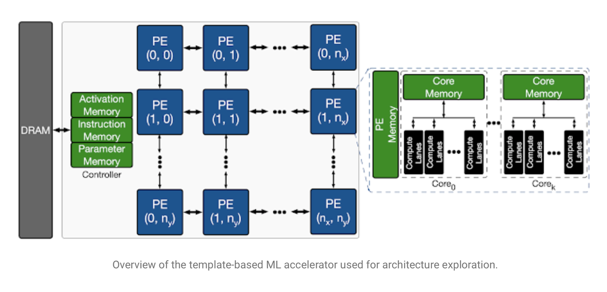
Given that the task is to design an AI chip, the architectures that the Apollo program is exploring are architectures suited to running neural networks. And that means lots of linear algebra, lots of simple mathematical units that perform matrix multiplications and sum the results.
The team define the challenge as one of finding the right mix of those math blocks to suit a given AI task. They chose a fairly simple AI task, a convolutional neural network called MobileNet, which is a resource-efficient network designed in 2017 by Andrew G. Howard and colleagues at Google. In addition, they tested workloads using several internally-designed networks for tasks such as object detection and semantic segmentation.
In this way, the goal becomes, What are the right parameters for the architecture of a chip such that for a given neural network task, the chip meets certain criteria such as speed?
The search involved sorting through over 452 million parameters, including how many of the math units, called processor elements, would be used, and how much parameter memory and activation memory would be optimal for a given model.
